
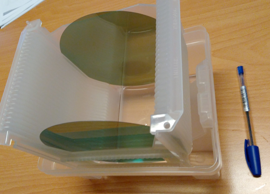
On 9 November 2026, Infineon announced that its Villach semiconductor factory in Austria had made functional power devices on 300 mm silicon-carbide (SiC) wafers using existing silicon manufacturing equipment. That is a far more meaningful milestone than simply growing a large crystal. It means at least some devices survived the manufacturing process and worked. But one crucial production number has not been released: yield.
Infineon describes the achievement as an industry first in a full-scale fab environment. The company displayed the processed wafer at electronica 2026 in Munich, which runs from 10 to 13 November. The 9 November announcement is verified; it is not a claim that customers can already buy 300 mm SiC devices in commercial volumes.
Why a working wafer changes the conversation
SiC can reduce switching and conduction losses in appropriately engineered high-voltage converters, from industrial drives and storage inverters to EV chargers and data-centre power systems. But SiC crystals and their manufacturing processes are difficult and expensive. Moving from 200 mm to 300 mm is not the equivalent of enlarging a photograph: crystal quality, thermal processing, wafer handling, defects, inspection and back-end assembly all need to remain under control across a substantially bigger surface.
Infineon says the larger diameter can provide about 2.3 times as many chips per wafer. That statement concerns potential die count: the simple ratio of wafer areas is (300/200)² = 2.25. It is not evidence of 2.3 times the number of saleable chips, 2.3 times the converter efficiency, or 2.3 times the factory output. Those would depend on defect density, usable edge area, process yield, device qualification, cycle time, equipment utilisation and cost.
This is the surprising engineering point. A demonstration with working devices proves feasibility, yet a fab production manager still needs the distribution of test results across the wafer, not merely a photograph of a successful specimen. Infineon has not disclosed electrical ratings, die-level yield, cost per good die, qualification results or a volume-ramp date for this 300 mm process.
Two different process breakthroughs — not one completed production line
Infineon’s release also describes a separate achievement in Dresden, Germany: it demonstrated the feasibility of applying its Cold Split separation technology to 300 mm SiC. In broad terms, the process aims to separate wafers from a crystal boule with less material lost and less processing time than conventional wire sawing. The material-saving claim comes from Infineon, not an independently reported manufacturing cost study.
Do not conflate the Dresden Cold Split trial with the Villach functional-device run. Wafer separation is an upstream materials challenge; producing qualified power devices is a downstream semiconductor-fabrication challenge. Both matter, but success in one does not establish high yield in the other. Infineon explicitly says the 300 mm industrialisation and ramp will be planned with customers and partners while its 200 mm SiC roadmap continues.
Video provenance: no authenticated original video specifically documenting this November 2026 Villach production run or the Dresden 300 mm Cold Split trial was established for this article. We therefore link the original manufacturer announcement, which includes its official wafer photographs, rather than attaching an unrelated semiconductor-factory video and implying it shows this process.
The number an engineer would ask for next
A device engineer would want breakdown voltage, on-resistance, switching-loss data, thermal behaviour, reliability qualification and process variation. A manufacturing engineer would want the wafer map, pass/fail limits, defect classification, actual good-die yield, equipment availability and cycle-time distribution. A buyer would want stable product specifications, qualified supply and a credible delivery schedule.
Infineon’s result is important because it moves 300 mm SiC power devices beyond a substrate-only claim and into working fabricated hardware. Yet it remains a process-feasibility milestone, not a proven reduction in the price of an industrial inverter next quarter. Independently published industry coverage likewise notes that commercial yields and the production timetable are still missing.
Where CANS engineering could make a measurable difference
CANS was not involved in Infineon’s development and makes no claim to have measured its yields or tested this wafer. The relevance is to the two kinds of industrial evidence that separate a promising technology from a repeatable result.
In a manufacturing plant: if a semiconductor, electronics or high-mix production line makes a similar process change, CansNEXUS MES/OEE and analytics, properly integrated with the site’s equipment and test systems, could tie material lot, machine programme revision, recipe, wafer or board identity, inspection outcome and downtime reason to a common history. It could reveal when the change improves good output per operating hour, not merely gross throughput. Test instruments, quality limits and traceable measurement systems remain the authority for whether parts pass.
In a plant using SiC power converters: CANS PLC/SCADA and energy-monitoring integration could time-align calibrated AC-input and DC-output measurements, auxiliary consumption, load, temperature, cooling-system flow and trip events. For an inverter or UPS, the useful result is a loss-and-efficiency curve over an agreed operating envelope, with appropriate measurement boundaries and uncertainty — not an efficiency estimate inferred from the wafer diameter. CansNEXUS trends, alarms and digital-twin views can support diagnosis and maintenance follow-up.
Limits and protection: these are monitoring and diagnostic functions. They cannot manufacture yield, make an unqualified semiconductor safe to deploy, or guarantee avoidance of converter faults. Protection against overcurrent, thermal runaway, insulation failure and dangerous switching conditions still depends on correctly engineered hardware protection, certified safety functions where required, maintenance and validated control logic independent of general AI dashboards.
What this milestone really proves
Making SiC devices work on 300 mm wafers is an impressive manufacturing step. Selling them consistently and economically will be a different test. The question for the next announcement is not simply whether the wafer gets bigger; it is whether the number of qualified devices per euro of production cost gets better.
For industrial power-converter measurement, production traceability or machine-data integration, contact CANS or enquire on WhatsApp.
Sources and image rights
- Infineon Technologies, 9 November 2026 — original Villach functional-device and Dresden Cold Split announcements; the 2.3-times claim is the manufacturer’s statement.
- Credence Research, 10 November 2026 — independent reporting discussing the manufacturing significance and the undisclosed yield and ramp.
- Silicon Showcase, 9 November 2026 — editorial distinction between functional devices, foundry availability and qualified volume production.
Featured photograph: two 150 mm SiC substrate wafers in a carrier, photographed by FDominec in March 2022, Wikimedia Commons; CC BY-SA 4.0, used unmodified. Illustrative only: these are neither Infineon’s 300 mm wafers nor images of its 2026 production achievement. The photograph is featured media and is not repeated within the body.
Recent Comments